第5章アルゴリズムのハードウェアによる実現:コンピューターシステム設計
The Memory Hierarchyメモリ階層
We have five items on our wish list for an ideal memory and, since there is no single technology that excels in all five, we must combine several technologies to come close to the ideal memory system. This ideal memory system must be fast, dense, persistent, large in capacity, and inexpensive. The technologies that we currently use have the following characteristics:
英語のヒント
理想のメモリに求める性質は五つある。五つすべてで優れた単一の技術はないので、複数の技術を組み合わせ、理想のメモリシステムに近づける必要がある。その理想とは、高速、高密度、データを持続的に保持でき、大容量で、安価なことである。現在使っている技術には、次の特徴がある。
• Technology 1: very fast but expensive, less dense, and volatile
• 技術1:非常に高速であるが、高価で、密度が低く、揮発性がある。
• Technology 2: faster and denser, but volatile and moderately expensive
• 技術2:より高速で高密度であるが、揮発性があり、ある程度高価である。
• Technology 3: persistent and inexpensive but slow
• 技術3:データを持続的に保持でき、安価であるが、低速である。
• Technology 4: persistent and very inexpensive but very slow
• 技術4:データを持続的に保持でき、非常に安価であるが、非常に低速である。
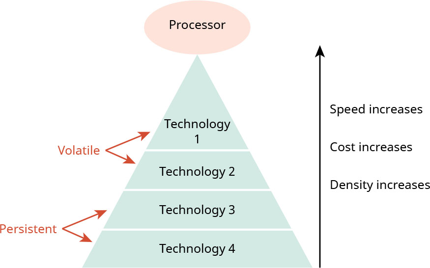
We need to get the best of all of them, and the best way to combine them must ensure that we have higher capacity from technologies 3 and 4 but make technologies 1 and 2 closer to the processor so that they can respond faster to the processor. The obvious way to do this is to use an arrangement of storage available on a computer system in the form of a triangle as shown in Figure 5.20. We call this design memory hierarchy.
英語のヒント
それぞれの長所を引き出す必要がある。最適な組み合わせでは、技術3と4で大容量を確保する一方、技術1と2をプロセッサの近くに置き、プロセッサへ速く応答できるようにする。わかりやすい方法は、図5.20のように、コンピューターで利用できる記憶装置を三角形の形に配置することである。この設計を、メモリ階層という。
attribution: Copyright Rice University, OpenStax, under CC BY 4.0 license · CC BY 4.0 · Source出典
Figure 5.20 Memory hierarchy makes the best use of all technologies. (attribution: Copyright Rice University, OpenStax, under CC BY 4.0 license)
図5.20 メモリ階層は、各技術を最も効果的に活用する。(出典:著作権 Rice University、OpenStax。CC BY 4.0ライセンス)
Table 5.3 gives the names of the technologies that we discuss later in this section. The processor is connected to the first cache using a set of wires called the bus. If the processor does not find what it wants, it goes to the next level, and so on.
英語のヒント
表5.3に、この節の後半で説明する技術の名前を示している。プロセッサは、バスと呼ばれる配線の集まりによって、最初のキャッシュに接続されている。必要なものが見つからなければ、次の階層へ進み、以後も同様に探す。
Technology Name 技術名 | Use Case 用途 | |
|---|---|---|
Technology 1 技術1 | Static random access memory (SRAM) スタティック・ランダムアクセスメモリ(SRAM) | Cache memory • Volatile • Very fast • Expensive • Small in size (from few KB to few MB) キャッシュメモリ• 揮発性• 非常に高速• 高価• 容量が小さい(数KB~数MB) |
Technology 2 技術2 | Dynamic random access memory (DRAM) ダイナミック・ランダムアクセスメモリ(DRAM) | Main memory • Volatile • Fast • Less expensive • Average in size (1GB to 128GB) 主記憶• 揮発性• 高速• 比較的安価• 中程度の容量(1GB~128GB) |
Table 5.3 Technologies Used for Storage in a Typical Computer System
表5.3 一般的なコンピューターシステムの記憶に使われる技術
Technology Name 技術名 | Use Case 用途 | |
|---|---|---|
Technology 3 技術3 | Solid-state drive (SSD) ソリッドステートドライブ(SSD) | Storage • Persistent • Slow • Cheap • Big in size (few GB to few TB) ストレージ• データを持続的に保持• 低速• 安価• 容量が大きい(数GB~数TB) |
Technology 4 技術4 | Hard disk drive (HDD) ハードディスクドライブ(HDD) | Storage • Persistent • Very slow • Very cheap • Several TB of storage ストレージ• データを持続的に保持• 非常に低速• 非常に安価• 数TBの記憶容量 |
Table 5.3 Technologies Used for Storage in a Typical Computer System
表5.3 一般的なコンピューターシステムの記憶に使われる技術
Memory Technologiesメモリ技術
Memory is volatile, at least for now, with research exploring other technologies for persistent memories, speed, storage, and expense. This covers technologies 1 and 2 and, therefore, they are closer to the processor. Technologies 1 and 2 cover two types of memories that both include random access memory (RAM), which allows the processor to access any part of the memory in any order. Technology 2 is called DRAM, and technology 1 is called SRAM. Let us explore each one in turn.
英語のヒント
少なくとも現在、メモリは揮発性である。持続的な保持、速度、記憶容量、費用の面から、ほかの技術も研究されている。ここに該当するのが技術1と2で、そのためプロセッサの近くに置かれる。技術1と2が扱う二つのメモリは、どちらもランダムアクセスメモリ(RAM)であり、プロセッサがメモリ内のどの場所にも任意の順序でアクセスできる。技術2はDRAM、技術1はSRAMである。それぞれを順に調べよう。
Memory: DRAMメモリ:DRAM
As you now know, the memory stores instructions and data, which are presented as 1s and 0s. One type of memory, dynamic random access memory (DRAM), consists of a large number of capacitors. A capacitor is a very small electrical component that stores an electrical charge. A capacitor can be in one of two states: either it holds a charge, in which case we say that a 1 is stored in this capacitor, or it does not hold a charge, which means a 0. With millions of capacitors, we can store a large number of 1s and 0s. This is what you find in the specs of your laptop; when you say that you have 32GB of RAM, it means there are about 32 billion bytes in memory. Each byte consists of 8 bits. Each bit requires a capacitor.
英語のヒント
すでに学んだように、メモリには、1と0で表された命令とデータが保存される。メモリの一種であるダイナミックランダムアクセスメモリ(DRAM)は、多数のコンデンサーで構成されている。コンデンサーは、電荷を蓄える非常に小さな電気部品である。コンデンサーには、二つの状態がある。電荷を保持していれば1を保存しているといい、電荷を保持していなければ0を意味する。何百万ものコンデンサーがあれば、多数の1と0を保存できる。ノートパソコンの仕様に示されるのは、この容量である。RAMが32GBあるとは、およそ320億バイトのメモリがあるという意味である。1バイトは8ビットで、各ビットに一つのコンデンサーが必要である。
Capacitors have a not-so-great characteristic though. When a charge is left on a capacitor for some time, the capacitor starts discharging and loses its charge. This means we lose the data stored in memory. Because of this, there is circuitry built inside the DRAM that, every few milliseconds, checks the capacitors and adds a charge to them. We call this the refresh cycle. It is done dynamically, hence the name dynamic RAM or DRAM.
英語のヒント
しかし、コンデンサーにはあまり好ましくない性質がある。電荷を蓄えたまましばらく置くと、放電が始まり、電荷を失う。つまり、メモリに保存したデータが失われる。そのため、DRAMには、数ミリ秒ごとにコンデンサーを調べて電荷を補う回路が組み込まれている。これをリフレッシュサイクルという。動的に行われるため、ダイナミックRAM、あるいはDRAMと呼ばれる。
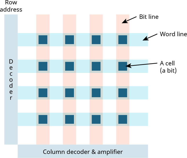
The capacitors are not standalone by themselves. Transistors are used with them to help organize those capacitors into rows (also called word lines) and columns (also called bit lines) for addressing specific bits. Figure 5.21 shows a simplified view of DRAM. The cell, which stores 1 bit, is made up of the capacitor and some transistors.
英語のヒント
コンデンサーは、単独で使うわけではない。特定のビットを指定できるように、トランジスタを組み合わせて、コンデンサーを行(ワード線ともいう)と列(ビット線ともいう)に整理する。図5.21は、DRAMを単純化した図である。1ビットを保存するセルは、コンデンサーといくつかのトランジスタで構成されている。
attribution: Copyright Rice University, OpenStax, under CC BY 4.0 license · CC BY 4.0 · Source出典
Figure 5.21 This simplified view of DRAM shows one bank. (attribution: Copyright Rice University, OpenStax, under CC BY 4.0 license)
図5.21 DRAMの簡略図で、一つのバンクを示している。(出典:著作権 Rice University、OpenStax。CC BY 4.0ライセンス)
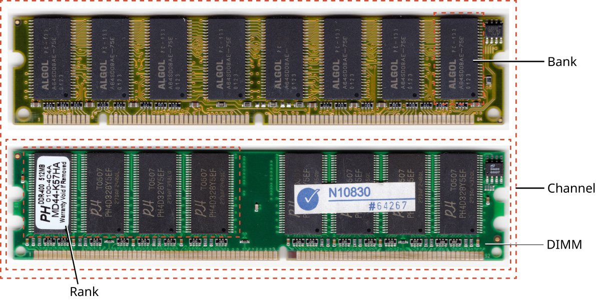
What is shown in Figure 5.21 is called a bank. Every few banks form a chip. Every few chips form a rank. A small memory board that contains several memory banks is a dual in-line memory module (DIMM). Several DIMMs form a channel. This organization is shown in Figure 5.22. The reason for having this organization is twofold. First, if we have one huge 2-D array of memory cells, it is too complex, slow, and power hungry, so dividing it into parts makes those parts simpler and that means faster and less power hungry. Second, if there are several memory addresses that need to be accessed and they fall into different banks, for example, the memory can respond in parallel.
英語のヒント
credit: modification of "168 pin and 184 pin DIMM memory modules" by Veeblefetzer/Wikimedia Commons, CC BY 4.0 · CC BY 4.0 · Source出典
Figure 5.22 DRAM memory banks can be organized into chips, ranks, DIMMs, and channels. (credit: modification of "168 pin and 184 pin DIMM memory modules" by Veeblefetzer/Wikimedia Commons, CC BY 4.0)
図5.22 DRAMのメモリバンクは、チップ、ランク、DIMM、チャネルへとまとめられる。(クレジット:Veeblefetzer/Wikimedia Commons「168 pin and 184 pin DIMM memory modules」を改変、CC BY 4.0)
You must have heard the term 64-bit machines, right? Most of our computer systems nowadays are 64 bit. One of the definitions of this term is that the connection between the processor and the memory has 64-bit width; its memory can send the data to, or receive data from, the processor in chunks of 64 bits.
英語のヒント
64ビットの機械という言葉を、聞いたことがあるだろう。現在のコンピューターシステムの大半は64ビットである。この言葉の定義の一つは、プロセッサとメモリの接続幅が64ビットあるということである。メモリは64ビットのまとまりごとに、プロセッサへデータを送り、またはプロセッサから受け取れる。
The curve that we saw in Figure 5.19 shows the slow speed increase of the DRAM, which affects the performance of the overall system. If the processor must go to the memory for every instruction and every piece of data, the overall system performance is very low; therefore, computer designers speed things up by using a faster technology together with the DRAM. This faster technology, technology 1 in Figure 5.20 is called the SRAM.